Sunday, October 30, 2016
In the previous articles we have seen basic operation and principle of a chopper.In this tutorial we will see Principle of Step-Down Chopper (Buck-Converter) with a neat sketch of circuit diagram
Don't Know What Is Chopper ? Click Here To Read It Now..
Buck-Converter ( Step-Down Chopper ) Principle & Working
In general, d.c. chopper consists of power semiconductor devices (SCR, BJT, power MOSFET, IGBT, GTO, MCT, etc., which works as a switch), input d.c. power supply, elements (R, L, C, etc.) and output load. (Refer below figure). The average output voltage across the load is controlled by varying on-period and off-period (or duty cycle) of the switch.
 Circuit Diagram") |
| Buck Converter ( Step-Down Chopper ) Circuit Diagram |
Buck-Converter ( Step-Down Chopper ) Operation
A commutation circuitry is required for SCR based chopper circuit. Therefore, in general, gate commutation devices based choppers have replaced the SCR based choppers. However, for high voltage and high-current applications, SCR based choppers are used. The variations in on and off periods of the switch provides an output voltage with an adjustable average value. The power-diode (DP) operates in freewheeling mode to provide a path to load-current when switch (S) is OFF. The smoothing inductor filters out the ripples in the load current. Switch S is kept conducting for period Ton and is blocked for period Toff. The chopped load voltage waveform is shown in figure.
 Output") |
| Buck Converter ( Step-Down Chopper ) Output |
During the period Ton, when the chopper is on, the supply terminals are connected to the load, terminals. During the interval Toff, when the chopper is off, load current flows through the freewheeling diode DF. As a result, load terminals are short circuited by DF and load voltage is therefore, zero during Toff. In this manner, a chopped dc. voltage is produced at the load terminals.
From output of buck converter figure, the average load-voltage E0 is given by
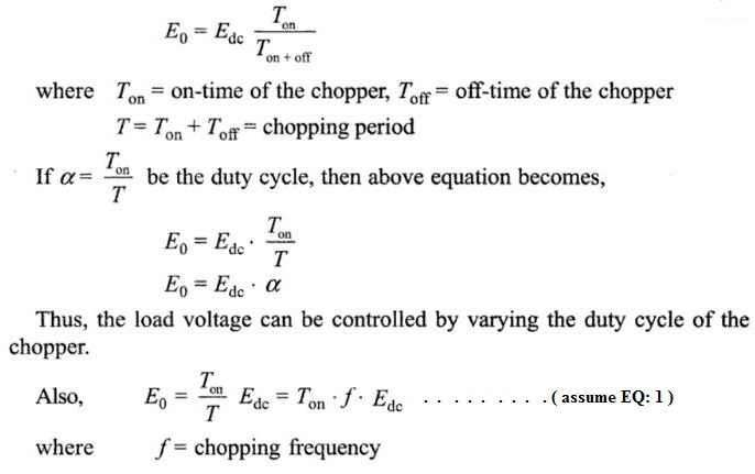
From Eq 1, it is obvious that the output voltage varies linearly with the duty-cycle. It is therefore possible to control the output voltage in the range zero to Edc.
If the switch S is a transistor, the base-current will control the ON and OFF period of the transistor switch. If the switch is GTO thyristor, a positive gate pulse will tum-it ON and a negative gate pulse will turn it OFF. If the switch is an SCR, a commutation circuit is required to turn it OFF.
